
| Experiments Menu | Teralab Main Menu |
|---|
This was an experiment to see if photocells could be made using my old Nanotech vacuum coater. Grey selenium is a light sensitive semiconductor and is easy to evaporate. Selenium photo-electric cells used to be used for photographic light meters. Selenium was also once also to make rectifiers and light sensitive drums for copying machines. I decided to try using it to make a thin film photo-electric cell. Selenium is quite easily available in pellet form as an element sample.
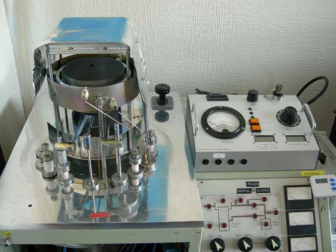
Above is a general view of the vacuum coater. The large cylindrical object on the left is an ion bombarder for cleaning and degasing. The substrate is at the top under the foil. The foil is there to minimize deposition on the bell jar. Evaporation was done thermally using a molybdenum boat.
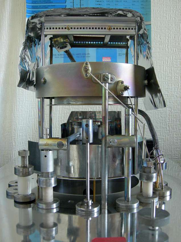
Above is a closer view of the coater setup. The small box on the spiral arm, top left is a coating thickness sensor. It uses a quartz crystal. As material is deposited onto the crystal, the oscillation frequency changes in a predictable manner. The thickness meter is an Edwards FTM2, which is obsolete and no longer supported. Luckily I have found that the modern Edwards E08668000 sensor crystals will work in it. The evaporation source is beneath the ion bombarder under a movable shutter.
For the first attempt (SPC1) a copper sheet was used as the substrate. The substrate was polished, chemically cleaned and then ion bombarded. 470nm of selenium was then deposited. The outer edges were then masked and 100nm of gold deposited. This is thin enough to be conductive but partially transparent to light. After a few hours, the film began blistering and peeling off. After a few days it was almost completely detached.
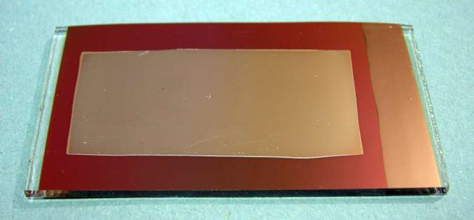
For the second attempt (SPC2) a sheet of window glass was used as the substrate. 30nm of gold was deposited followed by 5.5nm of cadmium. One end of the substrate was then masked and 200nm of selenium was deposited. The idea was that a CdO / Se junction would be formed. Finally, all sides were masked and 200nm of aluminium deposited as the back electrode. The device was found to have some sensitivity, but efficiency was very poor. Only 0.2μA was produced in room light. A photograph of SPC2 is shown above.
It was then decided to use selenium on tin oxide conductive glass (SPC3). A sheet of conductive glass was prepared as described on the Conductive Glass page. The substrate was 65mm x 34mm x 2mm thick. It was masked at one end and then selenium was deposited. It was then masked on all edges and 200nm of aluminium deposited as the back electrode. Sensitivity was again found to be very poor, but seemed to be improving with time. An attempt was made to anneal the selenium. The substrate was placed on a hot-plate, film side up, with another sheet of glass on top. The temperature was then raised to 110°C in air for 15 minutes. A change of colour was observed. From the front, it now looked brown/black rather than red as it had done before. The device now produced 0.7μA in room light and 1.2μA with a torch shone on it.
Based upon information in Chambers Materials Science and Technology Dictionary and sources on the internet, it seems that selenium can take on a number of different allotropic forms. Red selenium is an insulator, where as grey selenium is a semiconductor. The evaporation and condensation process appears to convert the grey selenium to red selenium. This can be at least partially reversed by heating.
It was decided to make another one, but with a gold back electrode (SPC4). One end of a newly made tin oxide conductive glass substrate was masked and 200nm of selenium deposited. All four sides were then masked and a further 200nm of selenium deposited, followed by 150nm of gold. The gold deposit looked grey on the selenium, but the surrounding selenium was cherry-red and partially transparent. The substrate was then heated to 150°C on a hot-plate. The colour of the selenium rapidly changed, taking on a more metallic look. With white light transmission, it still looked red. Connections were made using fine wire and silver loaded paint. It was found the the device was much more sensitive when connection was made to one end than at the other. The device then produced 2.4μA in room light and 250μA in bright sunlight. It is possible that there is a pin hole in the selenium film. This theory is supported by resistance measurements (494Ω at the sensitive end and 46Ω at the insensitive end).
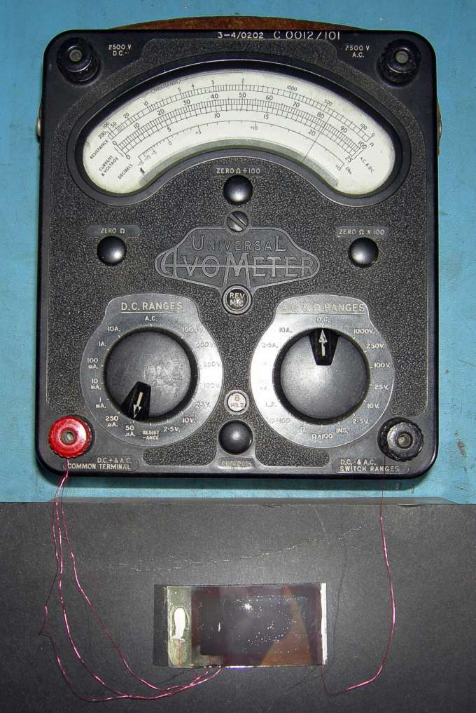
The photograph above shows cell SPC4 producing 42μA. A light meter indicates that the light was level was approximately 1000 lux. The active area of the cell is 10.2cm2. The sensitivity is therefore approximately 4nA/lux/cm2. This is about a tenth the sensitivity of commercial selenium photo-electric cells.
| Experiments Menu | Teralab Main Menu |
|---|